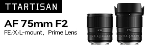
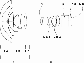
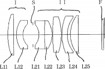
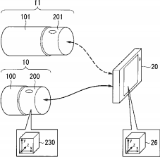
![]()
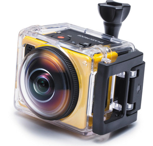
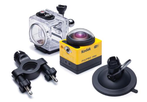
After years of financial troubles, Kodak reported $19 million earnings in third quarter:


Search PhotoRumors.com
 Custom Search
Categories
- 3 Legged Thing
- 7Artisans
- ACDSee
- Adobe
- Adonit
- Aftershoot
- Agfa
- Aiarty
- Akaralabs
- Alice Camera
- Alpa
- Alphagvrd
- Amphibico
- Antigravity
- Apple
- Aquatica
- Arca-Swiss
- Arri
- Artizlab
- ArtraLab
- AstrHori
- Atomos
- Aurora Aperture
- Avalanche
- BenQ
- Benro
- Blackmagic
- Blazar
- Brightin Star
- Broncolor
- C.P. Goerz
- Caira
- Camera Intelligence
- Canon
- Capture One
- Casio
- Caye
- Cheecar
- Chroma
- Contax
- Cooke
- Cosina
- CYME
- Deals
- Delkin
- DJI
- DK-Optic
- DuLens
- DxO
- DZOFilm
- Echolens
- Epson
- Escura
- Esquisse
- Excire
- Exposure Software
- Eye-Fi
- FieldMade
- Franke & Heidecke
- Freewell
- Fuji
- Funleader
- Future of Photo Equipment
- GE
- Gibellini
- Gizmon
- Godox
- GoPro
- Gura Gear
- H&Y filters
- HandeVision
- Harman
- Hasselblad
- Heipi
- Hobolite
- Holga
- Hollyland
- Hoya
- IDS Works
- Ikelite
- Ilford
- Impossible
- Insta360
- Irix
- Jintu
- JK Imaging
- JVC
- Kamlan
- Kase Optics
- Kenko Tokina
- Kinoshita
- Kipon
- Kodak
- Kolari
- Komamura
- Konica Minolta
- Kowa
- KUVRD
- Lailens
- Laowa
- Leaf
- Lee Works
- Leica
- Leitz
- Lenovo
- Lensbaby
- Lexar
- LG
- Light Lens Lab
- LightPix
- Logitech
- Lomography
- Lytro
- Macphun
- Mamiya
- Mandler
- Manfrotto
- Maven Filters
- Megadap
- Meike
- Metabones
- Metz
- Mevo
- Meyer Optik Görlitz
- Minolta
- Minox
- Mint Camera
- Mitakon
- Monster Adapter
- Mr.Ding
- Nauticam
- Neurapix
- Nextorage
- Nikon
- NiSi
- Nissin
- Nitecore
- Noktor
- Novoflex
- Oberwerth
- Olympus
- OM System
- ON1
- Opema Jena
- Other
- OWC
- Owlkrown
- Panasonic
- Peak Design
- Pelican
- Pentax
- Pergear
- Phase One
- PhotoEducate
- Phottix
- Pixii
- Pocket Wizard
- Polar
- Polaroid
- Polarpro
- PPPcameras
- PR reviews
- Praktica
- Profoto
- ProGrade
- ProGrade Digital
- Raspberry Pi
- Rayqual
- Red
- Ricoh
- Rockstar
- Rokinon
- Rollei
- Rolleiflex
- RRS
- Samsung
- Samyang
- SanDisk
- Schneider Kreuznach
- Sea&Sea
- SeaLife
- SG-IMAGE
- Sharp
- Sigma
- Sinar
- Sirui
- Sitina
- Skylum
- SLR Magic
- SmallRig
- Songdian
- Songraw
- Sonida
- Sony
- SPINN
- Squarehood
- Tamron
- Techart
- Thingyfy
- ThinkTank Photo
- Thypoch
- Tilta
- Tokina
- Top 10 Posts
- Topaz Labs
- Toshiba
- Tourist
- TTartisan
- Ulanzi
- Venus Optics
- Vi Vante
- Viltrox
- Vistilen
- Vivitar
- Voigtlander
- WANDRD
- Westcott
- Wideluxx
- Wise
- Xiaomi
- Yashica
- Yasuhara
- YI Technology
- YoloLiv
- Yongnuo
- Zeiss
- Zeniko
- Zenit
- Zhiyun
- Znonz
- Zonlai
- ZY Optics
Archive
Tags
5DayDeal 2015 CP+ show Adobe Photoshop CC BCN ranking Black Friday canonrumors Chinese lenses CIPA reports CP+ delay because of high demand delayed DxoMark test results film financial results firmware Fujifilm X-Pro1 Fujifilm X100 fujirumors Hasselblad X1D interview Kickstarter L-mount L-Mount Alliance Lightroom CC Luminar Neo ON1 Photo RAW Patents Pentax 645D Pentax full frame DSLR photo editing software Photokina 2012 Photokina 2014 Photokina 2016 Photokina 2018 price increase Rebates Roadmaps sonyrumors teaser To be discontinued... Topaz Labs Topaz Labs coupon code What's new on Kickstarter? What's next? What else is new?